Teacher
Graduated
- Chung-Lin Wu
- Chih-Chieh Wen
- Hsin-Hua Hu
- Ming-Lin Tsai
- Ming-Ching Wu
- Tsung-Hsien Lin
- Wang-Shen Su
- Other Docs
- Master
Doctor
- Kuo-Chen Wu
- Wei-Lun Sung
- You-Tao Li
- Chun-Hung Li
- Chih-Chun Li
- Chiung-Wen Lin
- Chia-Min Lin
- Chi-Tsung Hung
- Chih-Fan Hu
- Chih-Ming Sun
- Chia-Pao Hsu
- Chun-I Chang
- Heng-Chung Chang
- Chien-Lin C.C.
- Tsung-Lin Tang
- Yu-Chia Liu
- Yuen-Tung Liu
- Wen-Chien Chen
- Hsin-Yu Huang
- Yu-Che Huang
- Chun-Kai Chan
- Ming-Han Tsai
- Hsieh-Shen Hsieh
Master
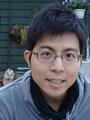
Chiung-Wen Lin
- Conference Proceedings: [1]H.-A. Yang, C.-W. Lin, and W. Fang, 2005, “Wafer Level Self-Assembly of Microstructures Using the Global Magnetic and Lifting Localized Induction Welding,” Transducers’05, Seoul, Korea.
- [2]C.-W. Lin, H.-A. Yang, L. Wang, and W. Fang, 2006, “Applied Through-wafer Interconnects and Anodic Bonding in SOI-MEMS Wafer-level Packaging,” The APCOT 2006 Conference, Singapore.
- [3]C.-W. Lin, H.-A. Yang, L. Wang, and W. Fang, 2006, “Applied 3D package and anodic wafer bonding in SOI-MEMS wafer-level packaging,” IMAPS-Taiwan 2006 Technical Symposium, Taiwan.
- [4]C.-W. Lin, H.-A. Yang, W. C. Wang, and W. Fang, 2007, “Thru-wafer Interconnect for SOI-MEMS 3D Wafer-level Hermetic Packaging,” Transducers’07, Lyon, France.
- [5]C.-W. Lin, C.-P. Hsu, H.-A. Yang, W. C. Wang, and W. Fang, 2008, “Implementation of SOG Devices with Embedded Through-wafer Silicon Vias Using a Novel Glass Reflow Process for Wafer-level 3D MEMS Integration,” IEEE MEMS’08, Tucson, AZ, USA.
- [6] C.-W. Lin, C.-W. Chang, Y.-T. Lee, Y.-C. Chen, S.-R. Yeh, H. Chen, T.-R.Yew, Y.-C. Chang, and W. Fang, 2008, “Glass Probe with Embedded Silicon Vias for 3D Integration,” EUROSENSORS 2008, Dresden, Germany
- [7] C.-W. Lin, C.-W. Chang, Y.-T. Lee, R. Chen, Y.-C. Chang, and W. Fang, 2009, “Glass Microprobe with Embedded Silicon Vias for 3D Integration,” IEEE MEMS’09, Sorrento, Italy.
- [8] Y.-T. Lee, C.-W. Lin, C.-M. Lin, S.-R. Yeh, Y.-C. Chang, C.-C. Fu, and W. Fang, 2009, “A 3D Glass Microprobe Array with Embedded Silicon for Alignment and Electrical Connection,” Transducers’09, Denver, CO, USA
- Journal papers: [1]H.-A. Yang, C.-W. Lin, and W. Fang, 2006, “Wafer level self-assembly of microstructures using the global magnetic lifting and localized Induction welding,” Journal of Micromechanics and Microengineering, Vol. 16, pp. 27-32.
- [2]H.-A. Yang, C.-W. Lin, C.-Y. Peng, and W. Fang, 2006, “On the selective magnetic induction heating of micron scale structures,” Journal of Micromechanics and Microengineering, Vol. 16, pp. 1314-1320.
- [3]C.-W. Lin, H.-A. Yang, W. C. Wang, and W. Fang, 2007“Implementation of three dimensional SOI-MEMS wafer level packaging using through-wafer interconnections,” Journal of Micromechanics and Microengineering, Vol. 17, pp. 1200-1205.
- [4]C.-W. Lin, C.-P. Hsu, H.-A. Yang, W. C. Wang, and W. Fang, 2008, “Implementation of silicon-on-glass MEMS devices with embedded through-wafer silicon vias using the glass reflow process for wafer-level packaging and 3D chip integration,” Journal of Micromechanics and Microengineering, Vol. 18, 025018.
- [5] C.-W. Lin, Y.-T. Lee, C.-W. Chang, W.-L. Hsu, Y.-C. Chang, and W. Fang, 2009, “Novel Glass Microprobe Arrays for Neural Recording,” Biosensors and Bioelectronics, Vol. 25, pp. 475-481.
Conference&Journal
- AutoBiography
Chiung-Wen (Jonas) Lin was born in Chang-Hua City, Taiwan. He received his Master degree in MEMS Institute, National Tsing Hua University in 2005. Right now he is pursuing a PhD degree in NEMS Insitute, National Tsing Hua University. He was a visiting student researcher of Berkeley Sensors and Actuators Center (BSAC) from 2009-2010 in Liwei Lin’s lab of UC Berkeley. His research interests include MEMS sensor design and integration, 3D integration based on TSV (Through-Silicon Via) technology, and novel application of nanomaterial.