Teacher
Graduated
Post-Doctor
Doctor
Master

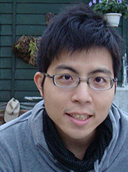
林炯文
- 現職:立錡科技
- 公司網頁:www.sitronix.com.tw/
- 博士畢業論文:具埋藏穿透矽晶片導線的微機電元件之開發及其於三維封裝與整合之應用
Conference&Journal
- Conference Proceedings:
[1]H.-A. Yang, C.-W. Lin, and W. Fang, 2005, “Wafer Level Self-Assembly of Microstructures Using the Global Magnetic and Lifting Localized Induction Welding,” Transducers’05, Seoul, Korea.
- [2]C.-W. Lin, H.-A. Yang, L. Wang, and W. Fang, 2006, “Applied Through-wafer Interconnects and Anodic Bonding in SOI-MEMS Wafer-level Packaging,” The APCOT 2006 Conference, Singapore.
- [3]C.-W. Lin, H.-A. Yang, L. Wang, and W. Fang, 2006, “Applied 3D package and anodic wafer bonding in SOI-MEMS wafer-level packaging,” IMAPS-Taiwan 2006 Technical Symposium, Taiwan.
- [4]C.-W. Lin, H.-A. Yang, W. C. Wang, and W. Fang, 2007, “Thru-wafer Interconnect for SOI-MEMS 3D Wafer-level Hermetic Packaging,” Transducers’07, Lyon, France.
- [5]C.-W. Lin, C.-P. Hsu, H.-A. Yang, W. C. Wang, and W. Fang, 2008, “Implementation of SOG Devices with Embedded Through-wafer Silicon Vias Using a Novel Glass Reflow Process for Wafer-level 3D MEMS Integration,” IEEE MEMS’08, Tucson, AZ, USA.
- [6] C.-W. Lin, C.-W. Chang, Y.-T. Lee, Y.-C. Chen, S.-R. Yeh, H. Chen, T.-R.Yew, Y.-C. Chang, and W. Fang, 2008, “Glass Probe with Embedded Silicon Vias for 3D Integration,” EUROSENSORS 2008, Dresden, Germany
- [7] C.-W. Lin, C.-W. Chang, Y.-T. Lee, R. Chen, Y.-C. Chang, and W. Fang, 2009, “Glass Microprobe with Embedded Silicon Vias for 3D Integration,” IEEE MEMS’09, Sorrento, Italy.
- [8] Y.-T. Lee, C.-W. Lin, C.-M. Lin, S.-R. Yeh, Y.-C. Chang, C.-C. Fu, and W. Fang, 2009, “A 3D Glass Microprobe Array with Embedded Silicon for Alignment and Electrical Connection,” Transducers’09, Denver, CO, USA
- Journal papers:
[1]H.-A. Yang, C.-W. Lin, and W. Fang, 2006, “Wafer level self-assembly of microstructures using the global magnetic lifting and localized Induction welding,” Journal of Micromechanics and Microengineering, Vol. 16, pp. 27-32.
- [2]H.-A. Yang, C.-W. Lin, C.-Y. Peng, and W. Fang, 2006, “On the selective magnetic induction heating of micron scale structures,” Journal of Micromechanics and Microengineering, Vol. 16, pp. 1314-1320.
- [3]C.-W. Lin, H.-A. Yang, W. C. Wang, and W. Fang, 2007“Implementation of three dimensional SOI-MEMS wafer level packaging using through-wafer interconnections,” Journal of Micromechanics and Microengineering, Vol. 17, pp. 1200-1205.
- [4]C.-W. Lin, C.-P. Hsu, H.-A. Yang, W. C. Wang, and W. Fang, 2008, “Implementation of silicon-on-glass MEMS devices with embedded through-wafer silicon vias using the glass reflow process for wafer-level packaging and 3D chip integration,” Journal of Micromechanics and Microengineering, Vol. 18, 025018.
- [5] C.-W. Lin, Y.-T. Lee, C.-W. Chang, W.-L. Hsu, Y.-C. Chang, and W. Fang, 2009, “Novel Glass Microprobe Arrays for Neural Recording,” Biosensors and Bioelectronics, Vol. 25, pp. 475-481.
- 學歷:
-
04/09-02/10 University of California, Berkeley, CA, United States
Visiting student researcher in Mechanical Engineering, and BSAC (Berkeley Sensors and Actuators Center)
Major field: Nanowire (TiO2) integrated MEMS device
Minor field: Dye-Sensitized Solar Cell (DSSC)
-
07/05-07/10 National Tsing Hua University, Hsin-Chu, Taiwan
(Expected) Ph. D. student in Institute of NanoEngineering and MicroSystem.
Major field: TSV for MEMS 3D integration.
Minor field: Glass micro probe array for neural recording
Dissertation proposal: Through-Silicon Via (TSV) in 3D Microsystem Integration.
- 07/03-06/05 National Tsing Hua University, Hsin-Chu, Taiwan
Master Degree in Institute of MEMS
Master thesis: Applied through-wafer interconnects and anodic bonding in SOI-MEMS wafer level packaging.
07/99-06/03 National Tsing Hua University, Hsin-Chu, Taiwan
Bachelor Degree in Power Mechanical Engineering
- 經歷:
- 97年國科會千里馬計畫補助
- 興趣嗜好:
- Interested in EVERY kind of outdoor activity!! Diecast model car collector.Travel around the world and experience the culture shock!
- 研究方向:
- My research focus on the 3D integration of microsystem based on TSV technology. Various MEMS device integrated with TSV was fabricated and tested successfully. The first device is metal TSV integrated SOI-MEMS device in 2008. The fabricated devices can be packaged at wafer level and are well suited for industrial field application. And this publication was also cited in Prof. M. Esashi topical review paper, “Wafer-level packaging of MEMS”. After that, I also invented another novel silicon TSV integrated SOG-MEMS (Silicon-on-Glass MEMS). Since the substrate is glass (insulator), so it well suited for inertia sensor which suffered from parasitic capacitance interrupt during output signal sensing. This silicon TSV embedded SOG-MEMS device also can be encapsulated at wafer level to lower the manufacturing cost. And this packaged device also passed the hermetic test standard (MIL-STD-883E). The final research topic is the novel glass microprobe integrated with silicon TSV for 3D assembled microprobe array. Taking advantages of insulation properties provided by glass, the glass microprobe is able to detect neural signal with good signal-to-noise ratio. And as before, this silicon TSV embedded glass microprobe can be stacked to form a 3D microprobe array.
After those exciting research I’d done in NTHU, Taiwan, I choose to continue my research abroad to broaden my research interest and field. I choose Univ. of California, Berkeley to serve as my another starting point of research. Here, I worked under advice of Prof. Liwei Lin in new research field – Nanotechnology. Right now I am working on titanium oxide nanosword integrated device. The first one is nanosword integrated MEMS device for SERS application. We implement the sharp tip provided by nanosword, which a strong local confined electromagnetic field will be produced under plasma excitation, to serve as a new SERS application. Another research field is the titanium dioxide nanosword for renewable energy application. Since there is a broad, flat, and highly reactive surface provided by nanosword, we try to integrate this new material in Dye-Sensitized Solar Cell (DSSC) for better dye absorption capability.
- E-Mail:
- jonaslin.ucb@gmail.com

